
Smart sensors on silicon wafer sorting equipment

Smart sensors on silicon wafer sorting equipment
Smart sensors on silicon wafer sorting equipmentUnder the "double carbon" goal, renewable energy sources such as solar energy are receiving more and more attention. With the competition and development of the photovoltaic industry itself, the demand for silicon wafer manufacturing processes and testing equipment is also continuing to increase.
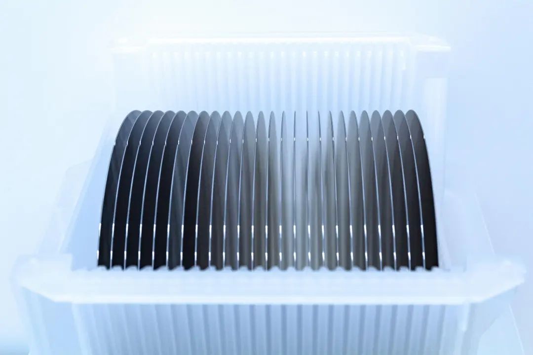
Silicon wafer sorting machine is an indispensable piece of equipment in the photovoltaic industry. It is mainly used to detect the geometric size and appearance defects (chamfering, chipping, dirt, cracks, etc.) of silicon wafers for fully automatic sorting. Wafer production companies apply this system to replace the previous manual inspection methods, which greatly improves the detection efficiency and fully meets the quality requirements of silicon wafer manufacturers. It also reduces the overall quality control costs of the company and downstream companies, and improves customers' performance in the industry. competitiveness.
In this issue, Xiao Ming will share AKUSENSE’s intelligent sensing solution for silicon wafer sorting machines;
The photovoltaic cell sheet detection and sorting machine can be divided into four mechanisms: the back transmission mechanism, the double feed grabbing mechanism, the grabbing cell sheet placement mechanism, and the double-sided feed box transmission mechanism.
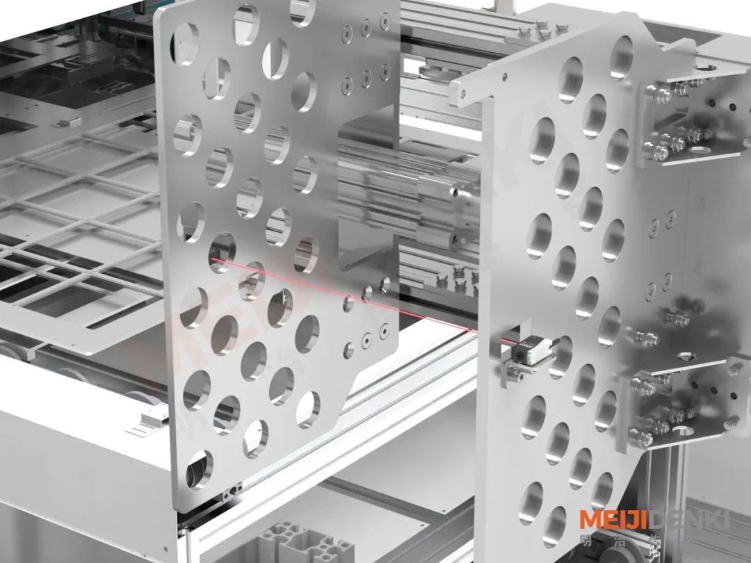
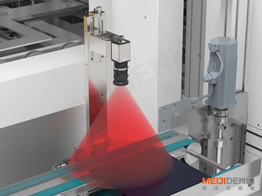
01 Robotic arm loading
Photoelectric sensor PTE-TEM10NR
Application scenarios:
The sensor positions the silicon chip. When the sensing pole piece is in place, the next step is triggered. The detection distance is 1m.
Detection difficulties:
1. It is required that the sensor will not be affected by the high reflection of the silicon wafer.
2. There is a stepper motor near the work station, which will generate electromagnetic fields during work and cause interference to the sensor.
3. The sensor is required to have an anti-vibration design
solution:
1. Use the through-beam photoelectric sensor PTE-TEM10NR series, with a detection distance of 1 meter, adjustable sensitivity, and easy installation and debugging.
2. The product uses high-quality light sources and has strong resistance to light interference.
3. The internal circuit is designed with precision technology and has strong anti-electromagnetic interference ability, and can still operate stably in a certain alternating electromagnetic field.
4. The shell is an integrated design of injection molding, with vibration resistance up to 50Hz (0.5mm amplitude) and superior performance.
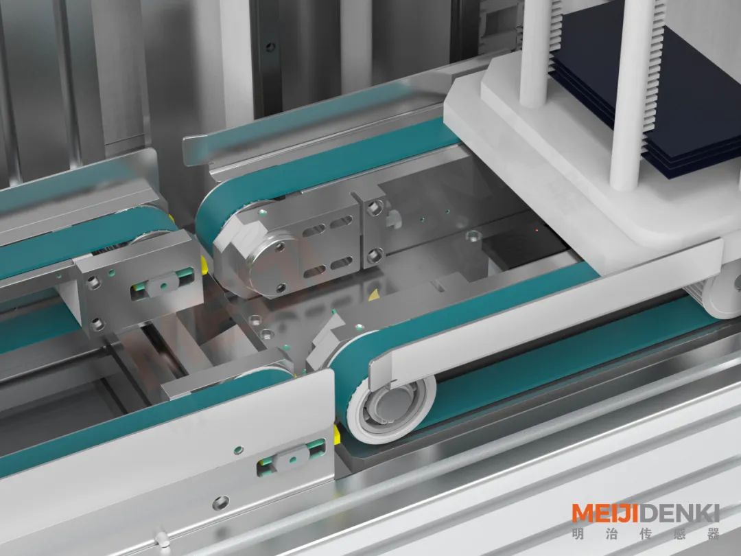
02 The silicon wafer is in place
CQ07-10NO flat capacitive proximity
Application scenarios:
The sensor detects the silicon wafer on the assembly line. When it detects that the silicon wafer is in place, the sensor sends a signal to drive the motor for transportation.
The sensor is required not to be affected by fluctuations in the flow line, and the detection distance can be adjusted at any time; it is not affected by the material of the silicon wafer, and it is a non-contact detection method.
solution:
1. Use the flat-shaped capacitive proximity sensor CQ07 series, which is not easily affected by the detection material (except insulating materials). The greater the dielectric constant of the detection material, the farther the sensing distance.
2. Detection distance 10mm, sensitivity adjustable in multiple turns
3. The sensor is only 7mm thick and has waist-shaped mounting holes for easy installation.
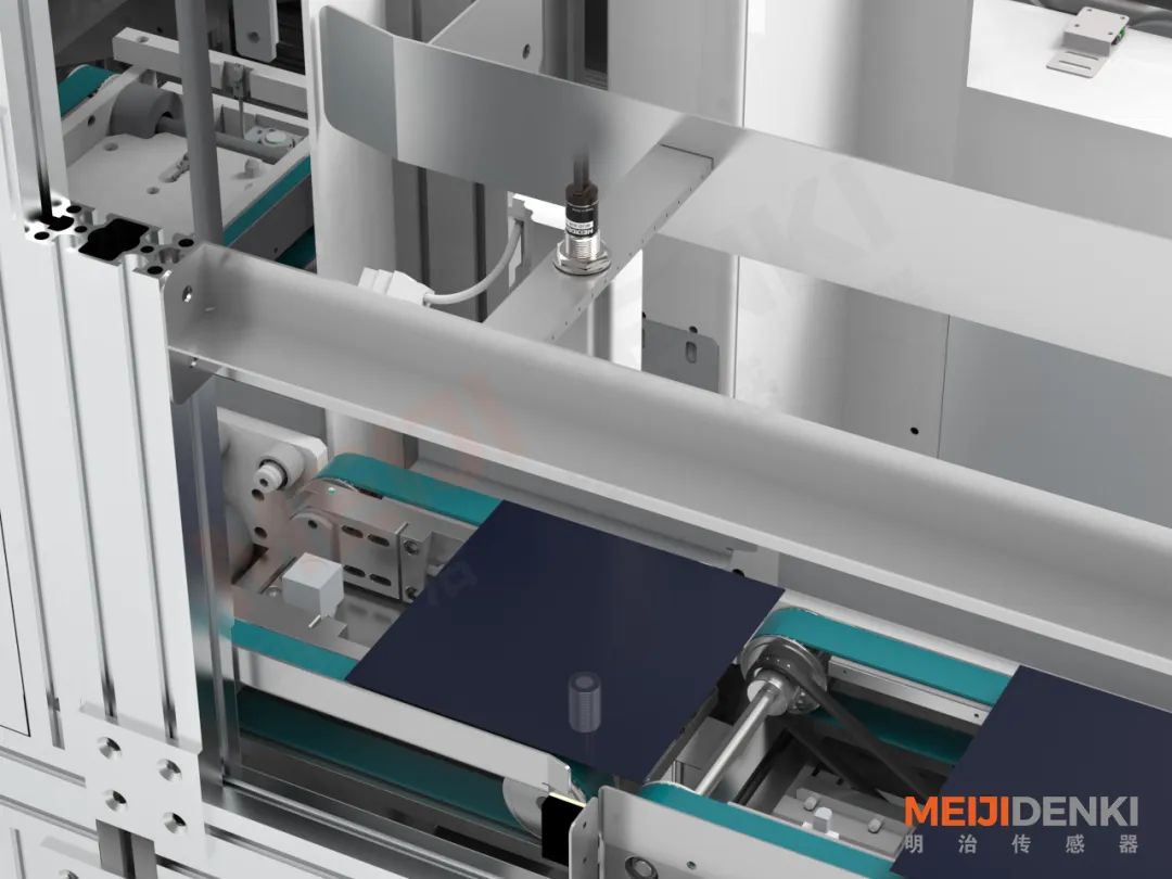
03 Single and double silicon wafer detection
MUD-60N-18-GL ultrasonic sensor
Application scenarios:
During the transmission of photovoltaic sheets, sensors need to be used to detect whether there are multiple sheets of materials. When the products are stacked or empty, a corresponding signal needs to be given, and the mechanism will reject the stacked materials or empty materials without proceeding to the next step.
1. The sensor is required to be compatible with silicon wafer detection needs of different thicknesses.
2. The conveying streamline rotates 1,200 times per second, which requires the sensor to be able to detect stably in the current high-speed operation scenario.
solution:
1. MUD series ultrasonic sensors can be used to detect empty materials and single and double sheets. The three detection modes are adjustable and have learning and teaching functions. They can be quickly debugged to adapt to the detection of various specifications of materials on site.
2. The detection distance can reach up to 60mm. Even if there are certain differences in the position of the material and jitter, it will not affect the actual detection effect.
3. The sensor supports jumper teaching, and teaching can be completed with simple settings, which is convenient and fast.
4. Using high-frequency detection algorithm, the response time can be up to 6.5ms, which can realize high-frequency detection
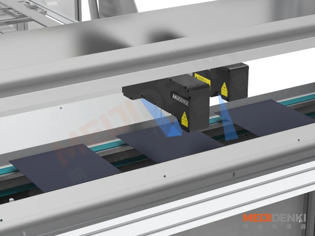
04 2D detection of silicon wafer chipping/surface defects
AKUSENSE non-standard visual solution
Application scenarios:
1. The visual field range is required to be about 100-150mm; the detection accuracy is required to be about 0.2mm, and everything that the human eye can see must be detected
2. The working distance is required to be within 400mm, and do not take up too much space.
3. The detection function requires the output of IO and serial port communication, and the generation of production record reports, requiring simple operation.
4. The detection beat requires 0.1s or less.
solution:
Machine vision is a key feature in silicon wafer sorters. In order to improve the detection accuracy and efficiency of silicon wafer sorters, helps equipment manufacturers achieve comprehensive control of silicon wafer quality by using high-quality light sources, professional cameras and precise algorithm solutions. control.
1. Achieve accuracy requirement 0.15±0.05mm
2. Working distance 300mm, small space occupation
3. Integrate the advantages of AI algorithms and traditional visual inspection to achieve new breakthroughs in visual inspection
4. Super model parallelism and image processing capabilities and industry-leading machine vision algorithm capabilities
5. A powerful software algorithm team that can develop according to customer customized needs
6. Professional technical service team to solve various technical problems
05 Silicon wafer flatness/thickness detection
Line laser sensor ESX series
Application scenarios:
1. Measure the thickness of the silicon wafer, the accuracy is single camera static data ≤ 0.2um
2. Measure the warpage of silicon wafers
3. Line scan laser supports IO external control and encoder triggering methods
solution:
1. It can achieve a repeatability accuracy of up to 0.1μm, fully meeting the current detection scenarios.
2. This product is specially designed for the photovoltaic industry. It uses imported light sources and light quantity adaptive algorithms to achieve high-precision measurement.
3. The product passes high and low temperature, vibration, impact and other tests before leaving the factory to meet most industrial application scenarios. Commonly used industrial interfaces
(Serial port, encoder, analog output, etc.) can be directly connected from the probe, easy to integrate
06 Regional security protection
BZL20-T1606NC safety light curtain
Application scenarios:
To prevent people from accidentally entering the equipment working area and causing injuries when the robot grasps silicon wafers, the response time is required to be less than 15ms and the detection is stable.
solution:
1. Choose ultra-thin light curtain BZL series, which is only half the thickness of conventional light curtains, leaving a larger operating space for the equipment.
2. Millisecond-level response speed, efficient and sensitive
3. Multiple choices, optical axis spacing 10/14/20/25/30/40mm, front light and side light optional, greatly improving the convenience of equipment design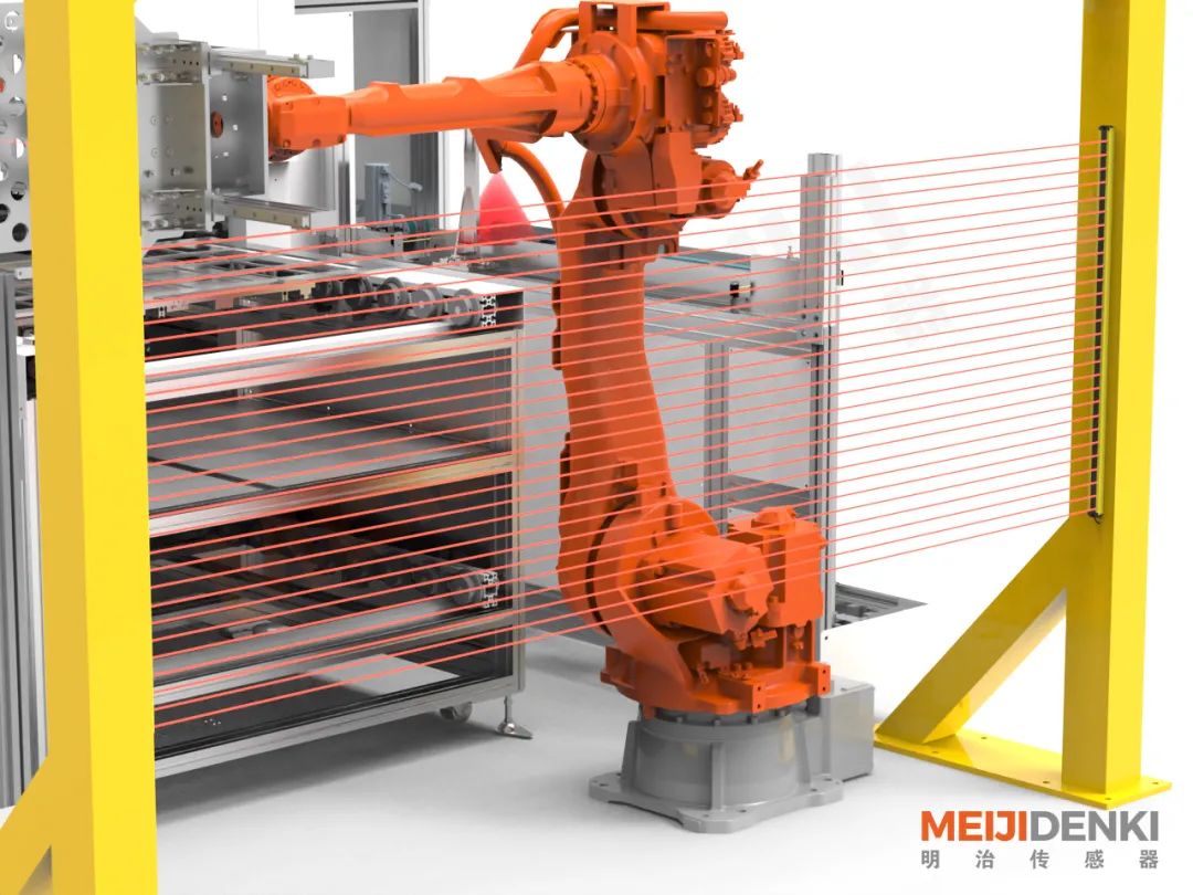
The trend of energy reform is imperative. Sensing is committed to riding on the wave of intelligent upgrading in the photovoltaic industry, combining its own advantages with in-depth industry needs, constantly iterating product functions and solution capabilities, and assisting the intelligent upgrading of the photovoltaic industry.
+86 18188641602

Akusense Technology Co., Ltd.