
Semiconductor etching equipment

Semiconductor etching equipment
Popular sensors used in semiconductor etching equipmentIf the chip is compared to a flat carving work, then the photolithography machine is the brush for drafting; the etching machine is the engraving knife; and the deposited film is the material used for engraving. The accuracy of photolithography directly determines the size of components, while the accuracy of etching and thin film deposition determines whether the size of photolithography can be actually processed. Therefore, photolithography, etching and thin film deposition equipment are the most important in the chip processing process. The three types of main equipment account for nearly 70% of the front-line equipment.
In recent years, our country has begun to carry out catch-up research and development in various types of equipment. Among the most technically difficult main equipment, etching machines are at the forefront of domestic substitution. Today, Xiao Ming will share the sensor application solution on semiconductor etching equipment.
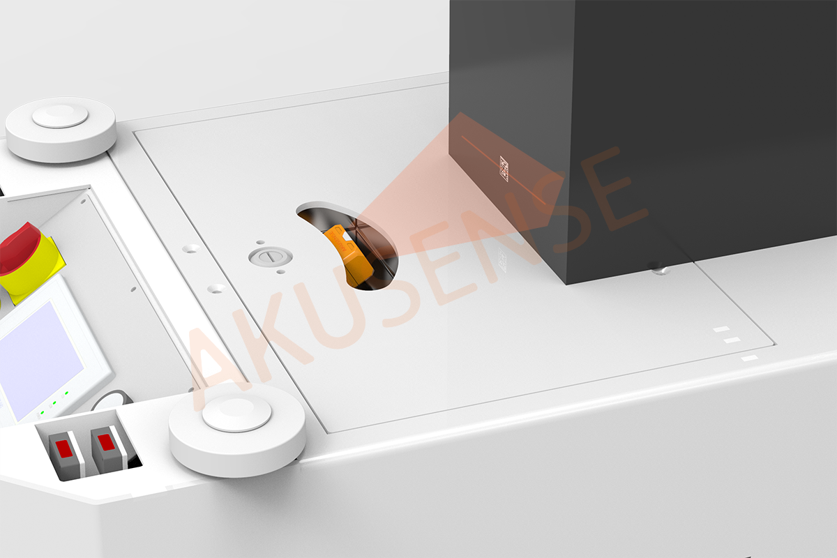
01 Carrier ID management
Intelligent code reader RCD-AI100-S
By automatically reading the universal barcode label attached to the FOUP box on the loading end, point-to-point precise management can be easily achieved and costs can be reduced. The algorithm is powerful and can read multiple barcodes at the same time.
02 Check whether the upper chip is present
Fiber optic sensor PG1+PT-32-DQ
Detect the presence of the top chip to determine whether it is full. In a small workstation structure, you need to choose a thin optical fiber to facilitate installation. The through-beam principle makes the detection more stable. With a PG1 amplifier, it can perform 13us Ultra-high-speed detection.

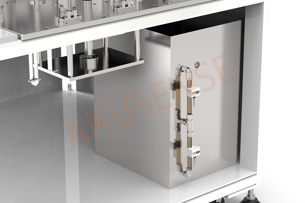
03 Control chemical liquid level
Liquid level sensor CE30-26NO
When there are bubbles in the pipe, the use of optical sensors may cause misjudgment. Therefore, a capacitive proximity sensor dedicated to pipe liquid level detection can be used. Even if bubbles are generated in the pipe, the detection can be stable and is not affected by the color and density of the liquid. , non-contact detection also eliminates the need for the sensor to consider chemicals reacting with the sensor.
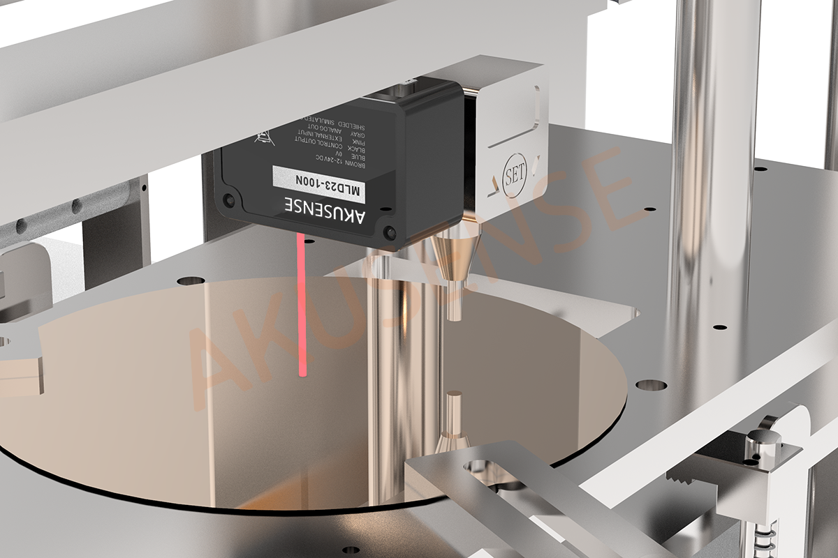
04 Target positioning and distance measurement
Laser displacement sensor MLD23-100N
This workstation needs to accurately measure the height of each wafer in real time. Meiji's laser displacement sensor has a large detection range of 65-135mm, which can monitor any position of the wafer in real time, with an accuracy of 0.01mm. The software function can be easily taught, improving Improves the convenience of debugging.
+86 18188641602

Akusense Technology Co., Ltd.