
How does 0.01mm high-precision visual inspection protect the "inch" of silicon wafers?
How does 0.01mm high-precision visual inspection protect the "inch" of silicon wafers?
The visual inspection system is playing the role of an "invisible quality inspector" - it uses a 0.01 millimeter level "golden eye" to guard the accuracy of every engraved line and marking point on the silicon wafer.
Today, as the semiconductor industry advances towards 3nm and 2nm processes, billions of transistors are densely packed on a 12 inch silicon wafer, with processing accuracy comparable to carving the Great Wall on a strand of hair.

In this microcosm war, the visual inspection system is playing the role of an "invisible quality inspector" - it uses a 0.01 millimeter level "golden eye" to guard the accuracy of every engraved line and marking point on the silicon wafer.
Scenario requirements
Measure the distance between the Mark point and the edge line;
Measure the width of a single engraved line;
Measure the distance between the engraved lines;
Measure the distance between four Mark points;
Measure the mutual distance between the outermost four lines;
Accuracy requirement<0.01mm
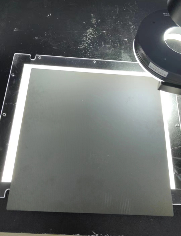
As the cornerstone of chip manufacturing, the Mark points etched on the surface of silicon wafers and the precision of micro scale engraved lines directly affect core processes such as photolithography alignment and wafer cutting. Traditional detection methods face three major challenges:
1. Accuracy bottleneck: The measurement error of manual micrometer reaches 0.05mm, which cannot meet the advanced packaging requirements;
2. Efficiency constraints: Contact measurement can easily damage the surface of silicon wafers, and single piece detection takes more than 5 minutes;
3. Data blind spot: unable to capture real-time changes in engraved line morphology, making it difficult to trace potential defects.
According to data from a semiconductor equipment manufacturer, wafer yield losses caused by detection errors can reach tens of millions of dollars annually. The breakthrough in industrial visual inspection technology has become the key to breaking through.
solution
Visual Solution: Precise Collaboration from Optical Design to Algorithm Breakthrough
2000W industrial camera: With a high resolution of 5496 × 3672 and a pixel size of 2.4 μ m, it meets the precision requirement of 0.01mm.
Far center lens WTL200-023X20: Far center design (distortion<0.1%), high depth of field (± 5 μ m), 0.23X magnification, ensuring measurement consistency within the field of view and avoiding measurement errors caused by angle deviation in traditional lenses.
Coaxial light source+polarizer: The coaxial light source uniformly illuminates the surface of the silicon wafer, and the polarizer filters the reflected light spot, solving the imaging overexposure problem caused by high reflectivity of the silicon wafer and improving the stability of edge detection.
Effect comparison: Traditional circular light sources are prone to producing light spots, resulting in blurred edges of the engraved lines and increased measurement errors.
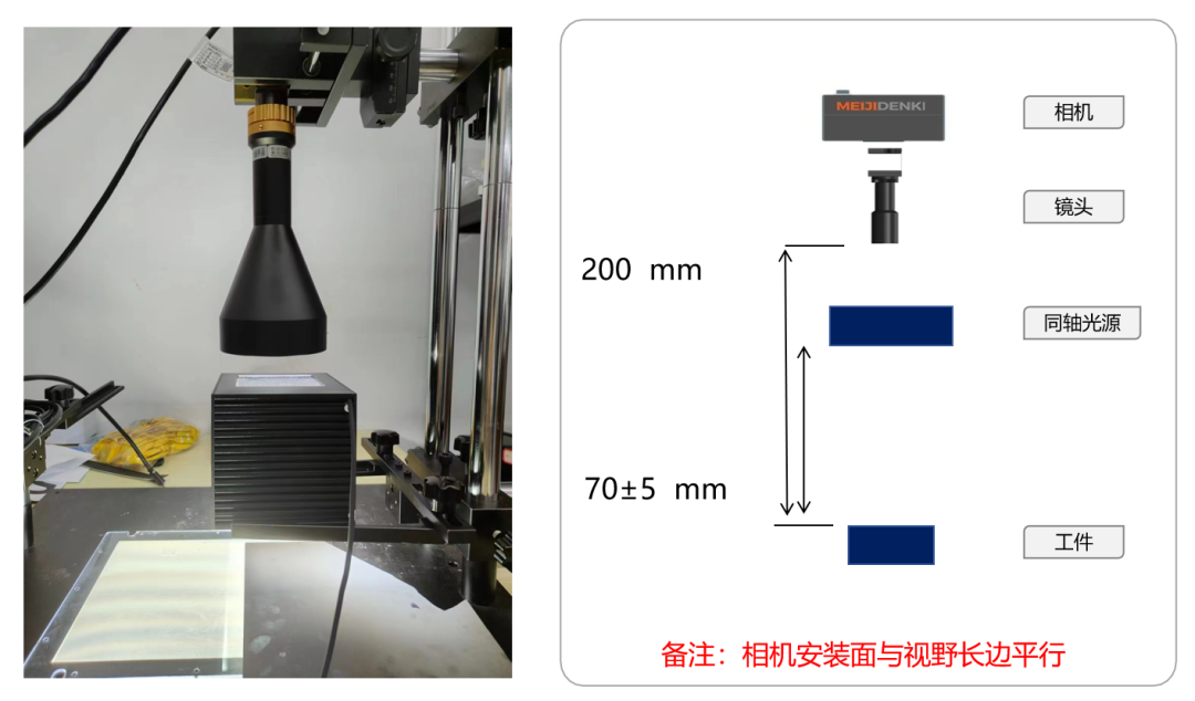
imaging effect
Overall detection effect
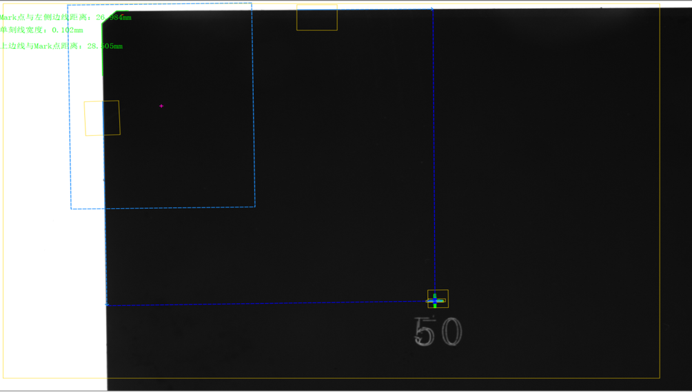
Distance between the upper line and the center of Mark

Mark point extraction effect
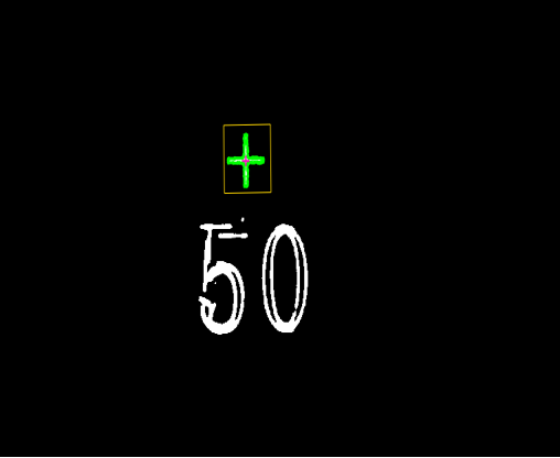
In the actual testing of a 12 inch silicon wafer production line, the system delivered impressive results:
Accuracy verification: The standard deviation of 30 consecutive measurements is less than 0.01mm, and the positioning error of the Mark point is only 0.6 μ m;
Beat optimization: By cropping the image size, the detection time is reduced to 180ms, which is 6 times faster than traditional methods;
Yield improvement: Defect detection rate reaches 99.98%, helping to increase production line yield by 0.15%.
The advantage of this solution configuration is not only reflected in its ultimate precision of 0.01mm, but also in its deep collaboration of hardware, optics, algorithms, and software to build a complete closed loop from "detection" to "intelligent decision-making".
+86 18188641602

Akusense Technology Co., Ltd.