
PCB visual inspection tool
PCB visual inspection tool
PCB visual inspection tool, accurately capturing [line sequence color], [missing components], and [solder joint details]
In today's 3C industry, visual inspection of PCBs has become a common solution, greatly improving production efficiency and product quality. However, with the increasing complexity and diversity of electronic product design, especially for PCB applications with special colors or similar backgrounds and diverse detection objects, traditional visual inspection solutions are often inadequate.
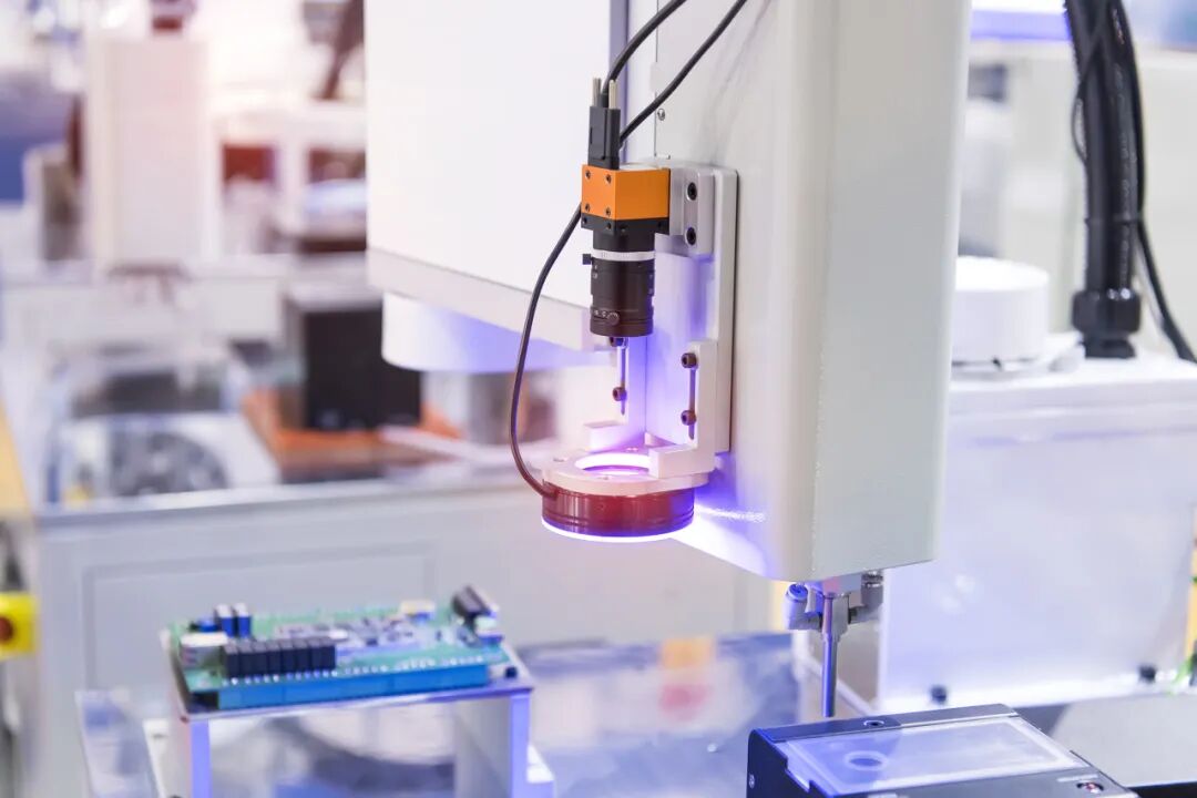
In the face of these challenges, targeted solutions are particularly important. Akusense Sensing, with its profound accumulation and innovative technology in the field of visual inspection, has successfully developed a visual system that can flexibly respond to various complex detection tasks. In this issue, Xiao Ming is here to share~
Scenario requirements
A certain electronic manufacturing customer needs to simultaneously complete three major tasks on the PCB board production line: line sequence color recognition, solder joint defect detection, and chip presence detection. Traditional manual inspection is inefficient and prone to missed detections. We have designed a high-precision and high-efficiency visual system that integrates traditional image processing and deep learning techniques to achieve full process automated detection

Difficulty analysis:
1. Line sequence detection: The black wire is consistent with the background, making it difficult to extract the image
2. Chip presence or absence: Some chips are pure black or consistent with the background color, resulting in fewer feature points being extracted;
3. Solder joint detection: solder joints have different shapes
solution
1. Ultra high definition imaging technology: Using a 12 megapixel, 4000 * 3000 resolution color camera, combined with a 16mm polarizer, it can capture every subtle line sequence, chip, and solder joint detail on the PCB board. Even under complex lighting conditions, it can ensure clear and non reflective images, providing a foundation for precise analysis in the future.
2. Multi dimensional lighting system: equipped with dual illumination solutions of perforated surface light and polarized strip light, providing customized lighting effects for different detection needs. The perforated surface light provides uniform background illumination and enhances contrast; Polarized stripe light effectively reduces reflection in areas such as solder joints, allowing defects to be exposed.
3. Intelligent algorithm driven: Meiji's visual platform integrates a series of advanced image processing and analysis algorithms, including edge detection, feature extraction, template matching, color segmentation, shape recognition, and optional machine learning algorithms. These algorithms can automatically recognize and determine whether the line sequence on the PCB board is correct, whether the chip exists, and whether the solder joint quality is qualified, achieving seamless conversion from image to data.
4. Efficient automation process: Unified control of cameras, lighting systems, and possible automation platforms is achieved through conventional four-way digital controllers. The preset automation process can be started with one click, automatically completing image acquisition, data processing, and result output, greatly improving detection efficiency and reducing manual intervention costs.
5. Customized inspection report: The generated inspection report provides detailed records of the inspection time, inspection results (including defect type, location, and quantity information), and image evidence. Users can customize the report format and content as needed, providing strong support for quality traceability and product improvement.
安装示意
1、将相机光源安装至合适位置开始调试相机
2、图像采集完成后,可以直接使用单目标特征匹配来定位特征(因打光效果质量较好,无需做图像处理)
3、使用三个彩色Blobo来识别三根线序颜色,防止焊接错误
4、与PLC做联动处理,将OK品与NG品打上相应标签,即完成整个检测流程
检测效果
① 线序识别效果
检测难点:黑色线材与背景一致,较难提取;
解决方法:裁剪图像,缩小检测范围;产品需保持平整放置槽内,翘起会导致成像打光不均,影响识别
② 焊点有无检测效果
检测难点:焊点特征的多样性
解决方案:使用深度学习算法来训练多种焊点形状,进行自动识别和分类,收集多张含正常/连锡/虚焊焊点的图像,标注缺陷区域进行训练
③ 芯片有无检测效果
检测难点:个别芯片为纯黑、或与背景色一致,导致提取特征点较少;产品翘起或不在槽内,导致打光不均;
解决方法:来料需保持产品在槽内无翘起,打光均匀;匹配增加采样点分布,确保稳定匹配;
在电子制造领域,技术的先进性与系统的可靠性是并驾齐驱的双轮。我们深知,对于PCB检测而言,技术的领先性固然重要,但系统的稳定性和可靠性更是基石。因此,在设计这套自动化检测解决方案时,我们始终将技术的可靠性放在首位。
此外,明治还注重系统的持续优化和升级,以应对不断变化的检测需求和挑战。通过不断的技术创新和算法优化,提升系统的检测精度和效率,为电子制造企业带来更加高效、精准的检测体验,支持用户成为行业领先者。
+86 18188641602

Akusense Technology Co., Ltd.